Working group Epitaxy
Workshop Epitaxy
AIXTRON
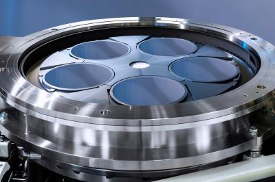
Epitaxy is a directed crystal growth method in which the atoms in the deposited layer are arranged in a specific, fixed crystal structure. In the production of electronic and optoelectronic components, these thin, single-crystal layers or structures with layer thicknesses of a few nanometers to micrometers must be deposited with the highest perfection. Gas-phase epitaxy, molecular beam epitaxy or liquid-phase epitaxy are used as epitaxy methods. Research and industry are working on different basic questions about layer growth – with high technological requirements for epitaxy methods, the corresponding reactor technology and the theoretical understanding of production, layer properties and application in devices. The epitaxy working group unites these diverse interests and focal points. At the same time, the working group is also working on very specific methods for characterizing extremely perfect and thin crystal layers.
Termin: Workshop Epitaxie
25.-27.11.2026 - Freiburg, IAF
Contact person
Prof. André Strittmatter
E-mail: andre.strittmatter@ovgu.de
Otto-von-Guericke Universität, Institute for Physics
Universitätsplatz 2, 39106 Magdeburg
Telefon: +49 33209449950
Overview of working groups